Why IR Curing is the Way to Go for Lead-Free Semiconductors
When you’re building biosensors, you’re basically playing a high-stakes game of “don’t melt the plastic.” You need to cure your adhesives and inks perfectly, but if you mess up the heat, you ruin the whole substrate. That’s why we stick with infrared (IR) lamps. They just make more sense.
Forget the Oven
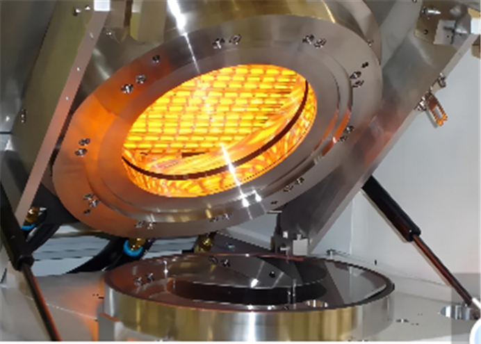
Most people think of big convection ovens. But here’s the thing: those ovens spend half their time just heating up the air around the part. It’s a waste of space and a waste of power. IR is different. It uses radiant energy, meaning the heat goesstraight into the material. No middleman. You get a much smaller footprint on your floor and you aren’t paying to heat a giant metal box of air. It’s just direct, efficient energy.
The “Goldilocks” Zone for Biosensors
Biosensors are finicky. Use a polymer that’s a few degrees too hot, and it’ll burn. Simple as that. We tune our lamps to hit specific wavelengths. This lets us cure the top layer of a sensor without accidentally cooking the circuitry underneath. It keeps everything flat and prevents that annoying warping that happens when materials get stressed by uneven heat.
Dealing with Lead-Free Materials
Switching to lead-free solder and adhesives usually feels like a headache. You’re dealing with higher melting points and weird viscosities. IR handles this with a “thermal punch.” It ramps up the heat in seconds. You get the intensity you need for lead-free gear, but you don’t have to leave your organic bio-components soaking in heat for an hour, which would normally degrade them. **But a word of caution:**IR is powerful. If your lamp spacing is off, you’ll get hot spots. You have to make sure your conveyor speed is perfectly synced with the wattage. If that belt slows down even a little? You’re going to scorch your wafers. And don’t forget to spec your cooling zones properly, or you’ll see the edges start to curl.